PCB和消费电子产品
Technical Cleanliness
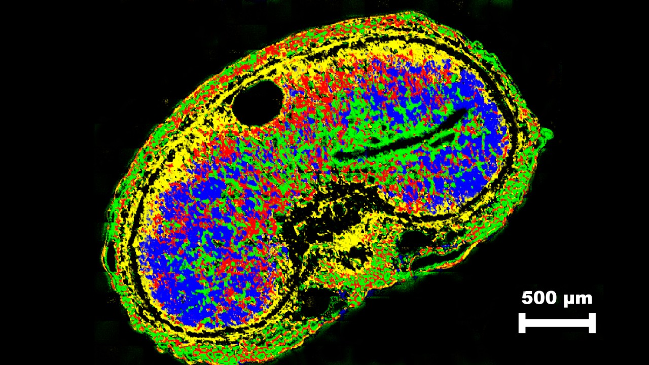
Root Cause Particle Analysis Using a Particle Trap and FT-IR Microscopy
无论是说出细灰尘还是微型塑料。微小的颗粒无处不在,除了它们对人类健康的影响外,它们是生产过程中产品损害和缺陷的主要原因之一。
无论是全能的,无论是技术清洁的地方,都必须进行可靠的残留污垢分析。FT-IR显微镜is a vital tool for tracking contamination routes and identifying the root cause.
In cooperation with other tools such as particle traps, entire spectral libraries of potential particle causes can be created. These can be searched in the event of defects and failures, to immediately clarify the reason for the damage.
故障分析
Contamination and Failure Analysis of a PCB by FT-IR Microscopy
一个PCBfailure is typically linked either to损害caused by thePCBmanufacturer during production, transport or due to environmental stresses. If such a failure occurs is often costs a大量的时间和神经。
为了节省这两个宝贵资源,FT-IR显微镜is a good choice, since it can contribute significantly towards understanding when and how a PCB damage occurred. Through careful microscopic chemical analysis, FT-IR microspectroscopy supports you in the following applications:
- Customer complaints
- Process troubleshooting
- Product failure and defect analysis
FT-IR显微镜分析CMOS芯片电路板
污染对产品质量有负面影响;特别是在微电子学领域,杂质是一个极为重要的话题。揭示污染的起源并启用快速故障排除是关键优势之一FT-IR显微镜.
红外光谱法的一个巨大优势是它为简单的视觉检查提供的化学对比度。这意味着,即使是无法检测到的污染也可以首先未被发现,也可以通过使用FT-IR光谱法发现。
传统上,它用于识别焊接和洗涤残留物,接触受损,电阻损坏或以任何形式的残留污垢分析

Elemental Distribution Analysis of Electronic Components with micro-XRF

微电子成分的复杂性增加。表面安装的设备(SMD)和集成电路(ICS)的大小和距离越来越小,电线和连接在印刷电路板(PCB)内的几层实现。因此,用于接近这类样品的分析方法既需要高空间分辨率,又需要研究样品深度的能力。
Micro-XRF是一种成像技术,将大约20 µm的空间分辨率与大多数金属的元素灵敏度相结合。M4龙卷风can therefore be a companion in the complete life cycle of electronic components, from R&D for novel designs and materials to recycling of precious metal components.
一个new Dimension for Failure Analysis
Consumer electronics contain a myriad of devices and sensors. As time goes on, the number of these components has increased exponentially while being placed in an ever-shrinking external package. X-ray Microscopy allow the non-destructing imaging of these items without the need for disassembly. This also presents an opportunity for next generation repair as failure mode can be diagnosed without having to open the case, a time-consuming process which often involves adhesives and specialty tools.
质量控制
用Micro-XRF快速,非破坏性质量控制镍涂层

电子镍镀(ENP)是一种自动催化化学过程,用于沉积一层镍磷(Ni-P)合金涂层。镍磷涂层厚度通常从1到40μm不等,具体取决于应用。电子镍涂层可以具有不同的磷含量,从而影响特定的冶金特性。磷范围通常从2%到15%的水平不等。镍磷涂层的关键好处之一是,它提供了一个非常一致的厚度,不依赖于部分几何形状。电子镀镍可以到达所有隐藏的表面,即使在最复杂的零件上,也可以提供完整的涂料覆盖范围。电子镍涂层例如在印刷电路板和连接器中使用。
When tight quality control of metal coatings is required, X-ray fluorescence (XRF) analysis is the best overall solution. The modern micro-XRF instrument, such as the BrukerM1 MISTRAL可以同时提供涂料厚度和涂料组成测量。
限制材料筛选
限制材料筛选with micro-XRF
随着电子设备的增加,电子废物也比以往任何时候都更快。近年来,欧盟和其他国家建立了多项法规,以促进电子废物的回收利用,并降低与电子废物产量增加相关的健康和环境风险。ROHS指令(限制某些危险物质的使用)是旨在通过限制其在电子设备中的使用来减少危险物质进入电子废物流的规则集之一。这些受限的材料包括重金属(铅,汞,bob综合游戏镉),六价铬,多溴阻燃剂(PBB和PBDE)和邻苯二甲酸酯。
X-ray fluorescence (XRF) offers a fast, non-destructive method of screening for these restricted elements. Small spot analysis is important for successful analysis, since the analysis beam must match the sample size which makesM1 MISTRALMicro-XRF ROHS筛选的理想选择。对于ROHS筛选,可选的准直仪在0.4毫米至1.5毫米之间可以对单个组件和电缆以及大量样品(金属,焊料,原材料)和大电路板进行准确分析。bob综合游戏

µXRD
一个nalysis of Soldered Joints with XRD

Electronic components are electrically and mechanically fixed to circuit boards with solder. The interaction of environment, flux and solder can lead to a myriad of crystallographic phases with differing properties. XRD goes beyond routine elemental analysis by positively identifying the phases that are present enabling proper diagnosis of failure mode.