PCBs and Consumer Electronics
技术清洁度
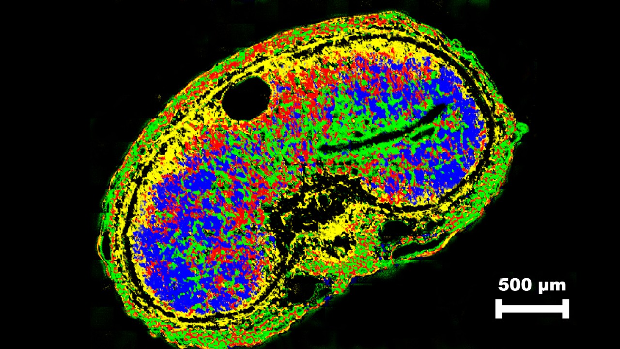
根本原因使用粒子陷阱和FT-IR显微镜分析粒子分析
No matter whether one speaks of fine dust or microplastics. Tiny particles are everywhere and apart from their impact on human health, they are one of the main causes of product damages and defects during production.
Wherever technical cleanliness is the be-all and end-all, a reliable residual dirt analysis is also a must.FT-IR microscopy是跟踪污染路线并识别根本原因的重要工具。
与其他工具(例如粒子陷阱)合作,可以创建潜在粒子原因的整个光谱库。可以在缺陷和失败的情况下搜索这些,以立即阐明损坏的原因。
Failure Analysis
FT-IR显微镜对PCB进行污染和故障分析
APCB失败通常链接到damage由PCB制造商在生产,运输或由于环境压力所致。如果发生这种失败,通常是费用lot of time and nerves.
In order to save both of these valuable resources,FT-IR microscopy是一个不错的选择,因为它可以为理解何时以及如何发生PCB损伤做出重大贡献。通过仔细的微观化学分析,FT-IR Microspectroscopicy在以下应用中为您提供了支持:
- 顾客投诉
- 处理故障排除
- 产品故障和缺陷分析
Analysis of a CMOS Chip Circuit Board by FT-IR Microscopy
Contaminations have a negative impact on the product quality; especially in the field of microelectronics impurities are an extremely important topic.Revealing the contamination's origin and enabling quick troubleshooting is one of the key advantages ofFT-IR显微镜。
One huge advantage of infrared spectroscopy is the chemical contrast it offers to a simple visual inspection. This means, that even contaminations that are undetectable have remained undetected first, can be discovered by using FT-IR spectroscopic methods.
It is traditionally used to identify soldering and washing residues, damaged contacts, damaged resistors or in any kind of Residual dirt analysis

用微XRF进行电子组件的元素分布分析

Microelectronic components are of increasing complexity. The size and distances of the surface mounted devices (SMD) and integrated circuits (ICs) are getting smaller and the wires and connections are implemented in several layers within the printed circuit board (PCB). Therefore, analytical methods to approach these sort of samples need both, a high spatial resolution and the capability to look into the depth of the sample.
Micro-XRFis an imaging technique which combines spatial resolution of roughly 20 µm with a very high elemental sensitivity for most metals.The M4 TORNADO因此,可以成为电子组件完整生命周期的伴侣,从新颖的设计和材料的研发到回收贵金属组件。bob综合游戏
故障分析的新维度
消费电子设备包含无数的设备和传感器。随着时间的流逝,这些组件的数量已成倍增加,同时将其放置在不断变化的外部包装中。X射线显微镜允许对这些项目进行无损成像,而无需拆卸。这也为下一代维修提供了机会,因为可以诊断出失败模式而无需打开案件,这是一个耗时的过程,通常涉及胶粘剂和专业工具。
Quality Control
Fast, Non-destructive Quality Control of Electroless Nickel Coatings with micro-XRF

Electroless nickel plating (ENP) is an auto-catalytic chemical process used to deposit a layer of nickel-phosphorus (Ni-P) alloy coating on a substrate. The nickel-phosphorus coating thickness varies typically from 1 to 40 μm depending on the application. Electroless nickel coatings can have varying phosphorus content which impacts specific metallurgical properties. The phosphorus range typically varies from 2% up to 15% level. One of the key benefits of the nickel-phosphorus coating is that it provides a very consistent thickness that isn't dependent on part geometry. Electroless nickel plating can reach all hidden surfaces to offer complete coating coverage even on the most intricate parts. Electroless nickel coating is used for example in printed circuit boards and connectors.
当需要对金属涂层进行紧密质量控制时,X射线荧光(XRF)分析是最佳的总体解决方案。现代的Micro-XRF乐器,例如BrukerM1 Mistralcan provide simultaneous coating thickness and coating composition measurement.
受限制的材料筛选
用Micro-XRF限制材料筛选
With the increasing presence of electronic devices, electronic waste is also being produced faster than ever before. In recent years the EU and other countries have established multiple regulations to promote recycling of e-waste and reduce the health and environmental risks associated with the increase in e-waste production. RoHS directive (Restriction of the use of certain Hazardous Substances) is one of those rule sets aimed at reducing hazardous material from entering e-waste streams by restricting their use in electronic equipment. These restricted materials include heavy metals (lead, mercury, cadmium), hexavalent chrome, polybrominated flame retardants (PBB and PBDE) and phthalates.
X射线荧光(XRF)为这些受限元素提供了快速,无损的筛选方法。小点分析对于成功分析很重要,因为分析光束必须与样本量相匹配,这使得M1 Mistralmicro-XRF perfect choice for RoHS screening. For RoHS screening selectable collimator between 0.4 mm and 1.5 mm allows accurate analysis on individual components and cables, as well as bulk samples (metals, solder, raw materials) and large circuit boards.

µxrd
与XRD的焊接接头分析

电子组件是电和机械固定在带焊料的电路板上的。环境,通量和焊料的相互作用会导致无数具有不同特性的晶体学阶段。XRD通过积极识别存在的阶段以适当诊断失败模式来超越常规元素分析。