LCD Screens and Optoelectronics
故障分析
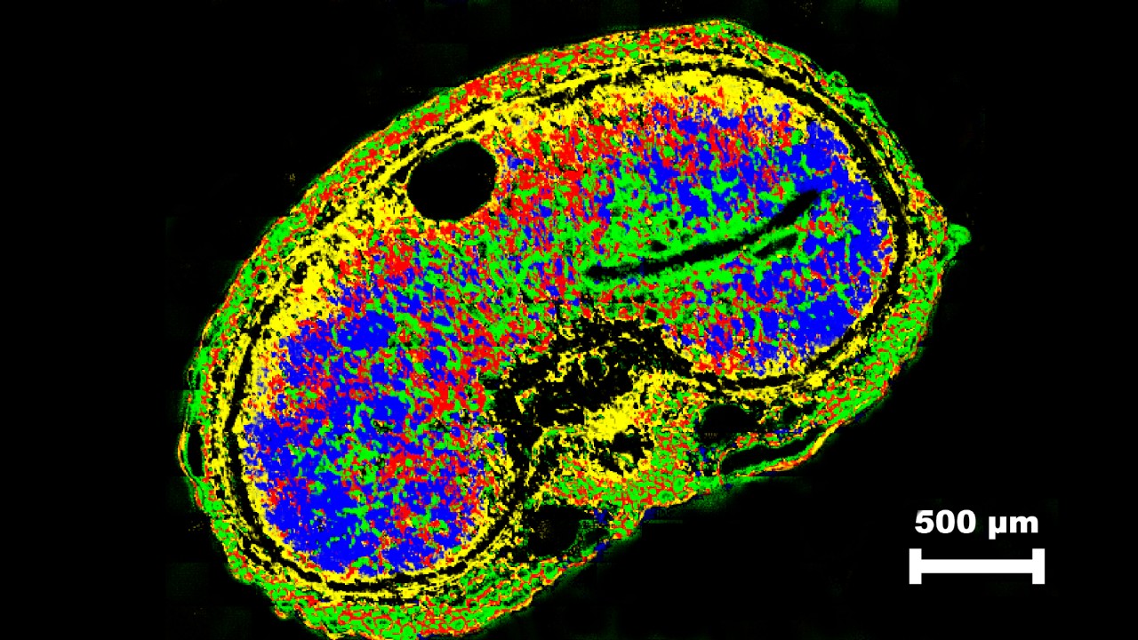
Defect Analysis of a CMOS Sensor by FT-IR Microscopy
The analysis of optoelectronic devices is quite complex since modern systems are highly miniaturized and composed of a multitude of materials. Especially the identification of microscopic contaminations is of particular interest as they can cause malfunctioning of the electronic device. Revealing the origin of the contamination and therefore allowing effective troubleshooting is one of the key applications ofFT-IR microscopy.
It allows users to obtain an IR-spectrum of very small structures with a high lateral resolution, thereby revealing the chemical composition of an defined part of the sample. This makes FT-IR an indispensable tool for quality control and failure analysis of electronic sensors and other optoelectronics. It can help characterize defects, damages, contaminations and much more. It can even stimulate product development by characterizing infrared sensors.

Quality Control
Investigate Contaminant Inside LCD Panel with Raman Microscopy
显示,LED,LCD和更多的光电部件被聚合物的保护层层压,或者只是粘在GLAS表面上。在这两种情况下,意味着材料是透明的,bob综合游戏共聚焦拉曼显微镜has the power to lookinside这样的组装。
Usually, very small contaminants like particles, fibers, dust and dirt are the culprits in such kinds of damages. Raman microscopy can not only find those microscopic impurities, it can identify them chemically to help discover the root cause of these product defects. Use it for damage analysis of:
- Screen and LCD assemblies
- Touchpanels
- Mounted sensors
Material Research
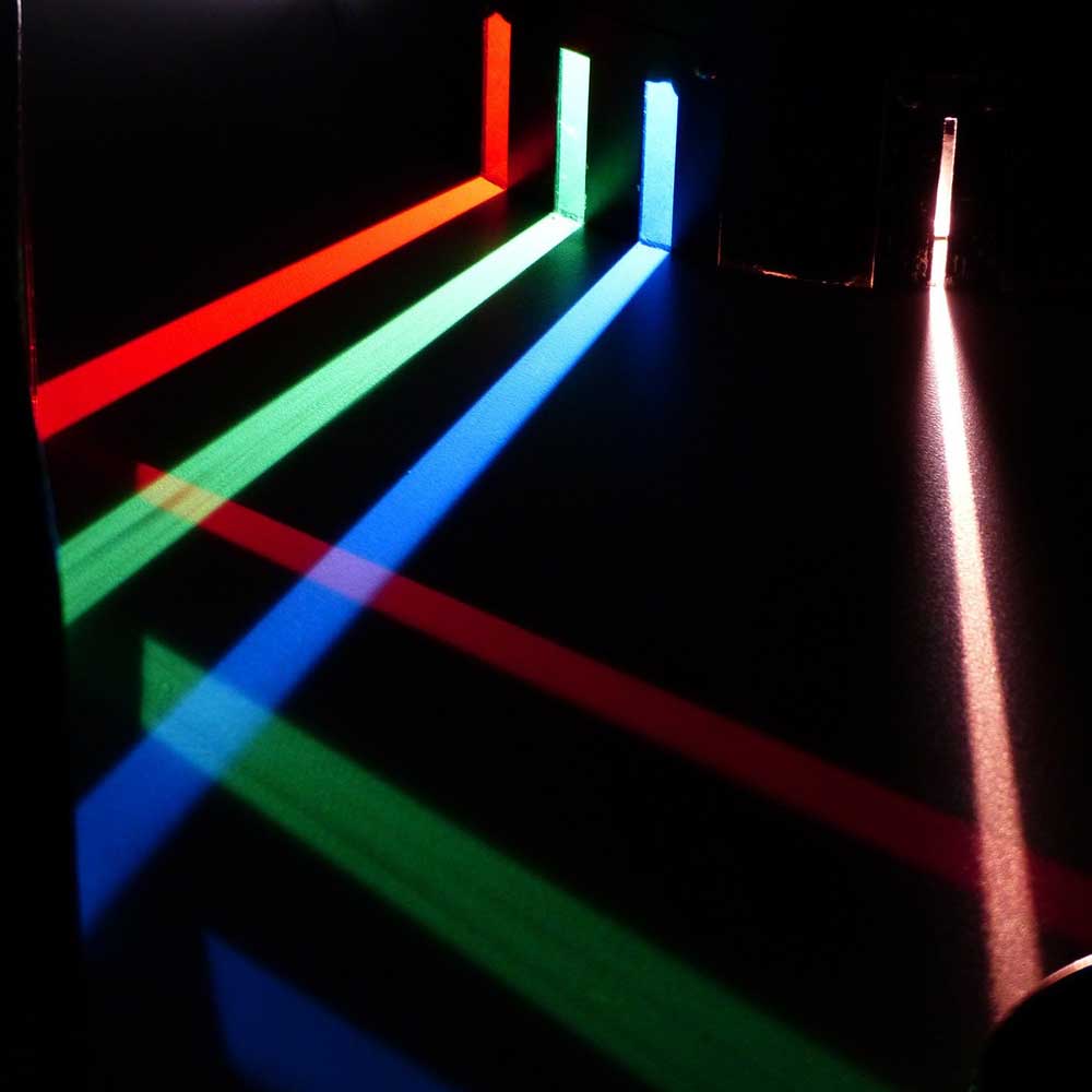
Sensor and Detector Characterization Using FT-IR

如今,探测器到处都是 - 在智能手机,温度计,相机,照明开关和许多其他设备中。但是,在这些探测器可以在我们的日常生活中开始工作之前,必须对它们进行彻底的特征和优化。
This is exactly where anFT-IR光谱仪can be broadly applied, examining detectors for the three basic parameters:
- 响应的光谱带宽(UV/VIS/IR/等)。
- Radiant power needed for a response
- Sensor response time
将FT-IR应用于VCSEL的开发以进行面部识别

Vertical Cavity Surface Emitting Lasers (VCSEL) are a special type of semiconductor laser diodes which, unlike conventional edge-emitting laser diodes, emit perpendicular to the chip surface. This makes them easy to package as emitter arrays with hundreds of emitters on a single chip, which can then be placed in a smartphone (e.g. for face recognition).
In the analysis of VCSELs,FT-IR spectroscopyhas proven to be a superior method compared to irradiance sensors and fast photodiodes. One of the many advantages is the possibility to determine emission spectra. Currently, research is focused on methods for characterizing VCSELs to support the theoretical modeling of VCSELs in basic research. You want to learn more?
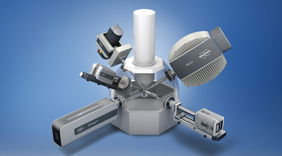
Correlating the Chemical Composition and Microstructure with Electrical and Optoelectronic Properties
Optoelectronic devices primarily rely on an optical stimulus to generate electrical pulses, and vice versa. They are commonly used as sensors or detectors in electronic devices.
SEM-based EDS和EBSD技术s are common analytical tools used in combination to investigate the correlation of the chemical composition and microstructure with optical, electrical and mechanical properties, and this down to the nanoscale. In-depth knowledge is possible with Bruker's advanced solutions forWDS, EDS, EBSD and TKD techniques定量测量相位和方向分布。例如,它允许研究特定晶体取向,晶粒或亚晶界对光电特性的菌株和性质的影响。也可以使用Bruker的原位相关研究Quantax EBSDandHysitron PI Series PicoIndenters.